
Normally sensor manufacturers have to choose between high speed and high resolution while also managing power consumption. Canon appears to be trying to find a way to balance all three needs with a new sensor patent.
As a sensor increases in speed or in resolution, it requires more power (both how much it draws and how a manufacturer has to manage the delivery). The latest patent application from Canon appears to be an attempt to make a sensor that is high resolution, high speed, and have lower power requirements.
If that sounds ambitious, it’s because it is.
“In recent years, multiple pixels of an imaging element have been advanced, and accordingly, there has been a tendency that a reading time of a pixel signal becomes longer,” the application reads. “Therefore, it is desired to increase reading speed.”
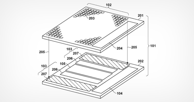
In the above diagram, you can see the stacked nature of the sensor, with the items marked 201 and 202 showing the lamination.
The solid-state image sensor 101 has a laminated structure including a first substrate 201 and a second substrate 202. The first substrate 201 includes a pixel unit 102, which is a pixel array in which unit pixels 203 are arranged in a matrix, and a control unit 204 that controls the pixels.
Dissecting the meaningful details of patent application language is always a challenge, but as explained by Canon News, the bottom layer has an ADC that converts the analog pixel values to digital and also acts as memory for both storing the values and also the amount of black level correction.
In the prior art, while the pixel signal can be read out at high speed, the number of vertical output lines in each pixel row increases, so that the number of constant current circuits to be connected increases and the power consumption increases. In particular, the increase in power consumption during Live View shooting greatly affects the number of shots that can be taken. Further, as the vertical output line of each pixel sequence increases, the scale of the correction circuit for correcting the offset to the pixel signal and the gain variation caused by the vertical output line increases. Correction circuit after the image sensor.
If it cannot cope with the increase in the vertical output line, it is necessary to mount a correction circuit on the image sensor. In this case, it is necessary to also mount a memory for storing the correction value, the power due to the read/write of the memory also increases, and the power consumption increases more and more.
The present invention has been made in view of the above-mentioned problems, and an object of the present invention is to provide an image pickup apparatus capable of achieving both high-speed reading of a pixel signal and reduction of power consumption.
It’s unclear if this idea actually works, and it’s certainly no guarantee that it will find its way into a product either in the near or far future. But it’s good to see Canon, a company that for years was ridiculed for its poor sensor technology, is once again pushing the envelope with new ideas.
(via Canon News)